EVENT
Friday, April 26, 2024
NanoSI Launch Event and Industrial Advisory Board (IAB) Meeting
ABOUT THE EVENT
We are thrilled to extend a warm welcome to you for the upcoming Launch Event and Industrial Advisory Board (IAB) Meeting of NanoSI on Friday, April 26th. This event promises to be an engaging platform where we will showcase the latest in groundbreaking research and developments. Moreover, it provides an ideal setting to explore collaboration opportunities aimed at reshaping the landscape of chip-level technology advancements and applications.
ABOUT NANOSI
Northeastern University’s Institute for NanoSystems Innovation (NanoSI) is a global hub focused on pioneering semiconductor exploration, learning, and innovation. We’re also an open center for industry-university collaborative research. Our industry-driven research spans a broad range of MEMS, semiconductor devices, circuits, and systems, enabling innovations in many areas including sensors, wearable and implantable electronics, 5G/6G communications, and wireless IoT devices.
DATE
Friday, April 26, 2024
TIME
8:30AM ET—7:30PM ET
LOCATION
8th Floor EXP Building,
815 Columbus Avenue,
Boston, MA 02120
CONTACT
w.zhang@northeastern.edu
AGENDA
08:30
Registration and Continental Breakfast
09:00-09:30
Welcome and Opening Remarks

David Luzzi
Speaker
Senior Vice Provost for Research at Northeastern and Vice President of the Northeastern University Innovation Campus in Burlington, Massachusetts (ICBM)

David Horsley
Speaker
Co-Director of the Institute for NanoSystems Innovation; Professor, Northeastern University

Matteo Rinaldi
Speaker
Co-Director of the Institute for NanoSystems Innovation; Professor, Northeastern University
09:30-10:00
Keynote Speech

Dana Weinstein
Keynote Speaker
Associate Professor of Electrical and Computer Engineering,
Purdue University and Special Advisor for CHIPS R&D at the Executive Office of the President, OSTP
10:00-10:30
Faculty Spotlight
Fully Integrated Miniaturized Microsystems for Biomedical Applications

Soner Sonmezoglu
Faculty Spotlight
Assistant Professor of Electrical and Computer Engineering, Northeastern University
10:30-10:45
Coffee Break
10:45-11:00
Oral Presentation:
Piezoelectric RF MEMS/NEMS for IoT, 5G, and sensing applications
Luca Colombo, PhD
Assistant Research Professor, Electrical and Computer Engineering, Northeastern University
ABSTRACT:
An overview of the most recent technological breakthroughs developed within Northeastern University in terms of materials, design, and manufacturing of piezoelectric Radio Frequency (RF) micro- and nano- electromechanical systems (MEMS/NEMS) for advanced Internet of Things (Iot), 5G and beyond-5G, and sensing applications.

11:00-11:15
Oral Presentation:
Subharmonic tags for far-field ultra-sensitive sensing applications
Hussein Hussein, PhD
Postdoctoral Research Associate, Northeastern University
ABSTRACT:
Optical frequency combs, featuring evenly spaced spectral lines, have been extensively studied and applied to metrology, signal processing, and sensing. Recently, frequency comb generation has been also extended to MHz frequencies by harnessing nonlinearities in microelectromechanical membranes. However, the generation of frequency combs at radio frequencies (RF) has been less explored, together with their potential application in wireless technologies. In this work, we demonstrate an RF system able to wirelessly and passively generate frequency combs. This circuit, which we name quasi-harmonic tag (qHT), offers a battery-free solution for far-field ranging of unmanned vehicles (UVs) in GPS-denied settings, and it enables a strong immunity to multipath interference, providing better accuracy than other RF approaches to far-field ranging. Here, we discuss the principle of operation, design, implementation, and performance of qHTs used to remotely measure the azimuthal distance of a UV flying in an uncontrolled electromagnetic environment. We show that qHTs can wirelessly generate frequency combs with μWatt-levels of incident power by leveraging the nonlinear interaction between an RF parametric oscillator and a high quality factor piezoelectric microacoustic resonator. Our technique for frequency comb generation opens new avenues for a wide range of RF applications beyond ranging, including timing, computing and sensing.

11:15-11:30
Oral Presentation:
Machine Learning and Generative AI for Automated Synthesis of Analog Integrated Circuits
Jian Gao
PhD Student at Northeastern University
ABSTRACT:
Artificial Intelligence (AI) has significantly transformed the landscape of Electronic Design Automation (EDA). This transformation is especially pronounced in the automation of analog circuit design—a long-standing challenge—where AI-driven methods have dramatically accelerated the design cycle. In this talk, we will explore the entire analog EDA workflow, with a focus on topology generation and circuit parameter optimization. For circuit parameter optimization at the pre-layout stage, we introduce a reinforcement learning (RL) framework that integrates crucial domain knowledge, such as circuit topology and couplings between specifications. By employing a multimodal network, our approach achieves human-level design precision (~99%) and surpasses the efficiency of existing leading methods by 1.5 times. It also demonstrates superior generalization to unseen specifications and excels in optimizing circuit performance. Building upon this, we enhance the training sampling efficiency of our RL framework by synergistically combining Bayesian optimization (BO) and RL to significantly accelerate the RL agent’s learning process and ensure robust design solutions across process, voltage, and temperature (PVT) variations. Looking ahead, we envision a plethora of open research opportunities to push the boundaries of AI-driven analog EDA.

11:30-12:00
Oral Presentation:
Nano-Watt Power RF Communication and Energy Harvesting Circuits for IoT
Ankit Mittal
PhD Student at Northeastern University
ABSTRACT:
The next generation of intelligent wireless technology, expected to support over a trillion IoT devices, demands reliable connectivity. The challenging wireless channel conditions necessitate additional IoT radio frequency (RF) infrastructure for reliable communication. In an increasingly congested IoT network, radios are forced to stay active, draining energy while awaiting an available channel. Moreover, the limited security in IoT devices makes them vulnerable to resource-exploiting security attacks. Addressing these challenges, especially in energy-limited systems like batteries, is significant with conventional architectures consuming milliwatts of power.
In this presentation, I will discuss circuits designed in 65-nm CMOS technology for a robust, energy-efficient, and spectrum-aware IoT infrastructure, integrating “opportunistic” energy harvesting. We have successfully demonstrated wireless transmission to a Wake-up Radio up to 12 feet at 915 MHz, achieving -55 dBm sensitivity with only 10 nW power consumption and interference resilience. Our ultra-low-power closed-loop distributed beamforming technique can harvest RF energy with an n2 boost in received signal strength by correcting for frequency and phase offset between transmitters. Our wireless power transfer infrastructure consumes less than 30 nW. Additionally, I will explore future directions, focusing on the “deploy-forget” approach for self-powered IoT systems.

11:45-12:30
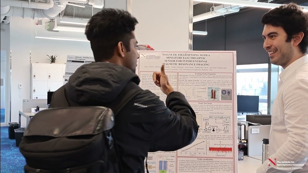
Morning Poster Session
13:00-14:00
Lunch
14:15-14:30
Oral Presentation:
Detection of Hardware Trojans through On-Chip Temperature Sensors
Thomas Gourousis
PhD Student at Northeastern University
ABSTRACT:
In this talk, an anomaly detection approach with non-invasive on-chip temperature sensing for Hardware Trojan detection will be presented, which is also coupled with a proposed anomaly detection technique using an autoencoder-based machine learning (ML) algorithm. In a case study, the developed algorithm identifies the Hardware Trojan with over 90 % accuracy for a Trojan power consumption that is as low as 2.5 % of the circuit under test. Besides identifying the Trojan, the algorithm can also provide information about the location of the Trojan on the chip. Furthermore, experimental results will be showcased from an on-chip temperature sensor prototype chip. A prototype chip of the proposed temperature sensor was fabricated in a standard 65-nm CMOS process. A measured sensitivity of 21.1 mV/μW is achieved over a dynamic range of 34 μW. The proposed on-chip anomaly detection approach with machine learning is under development as a solution for enhanced hardware security in modern electronic systems, particularly for Internet of Things applications.

14:30-14:45
Oral Presentation:
AI and Digital Twin Enabling Future Semiconductor Manufacturing
Haiyang Yun
PhD Student at Northeastern University
ABSTRACT:
Manufacturing advanced semiconductor devices with appropriate yield is challenging and complex because of intricate geometries, material variations, and process drift. It’s crucial to explore novel methodologies to enable innovative manufacturing beyond current limits for future semiconductor devices. We propose a Digital Twin methodology poised to revolutionize process development, leveraging proven models and a fusion of Artificial Intelligence (AI) with physics. Our approach not only provides quantitative information yielding actionable insights but also ensures scalability to High-Performance Computing (HPC) infrastructures and is compatible with secure processing protocols, including federated learning for secure data sharing and encrypted data processing methods. Illustrating our approach, we have successfully trained Deep Neural Network (DNN) models capable of predicting outcomes for DUV nanolithography, Plasma Etch processes, and printed electronics.
Furthermore, we have created tools facilitating autonomous measurements on complex CD metrology data, resilient to background variations. A notable advancement is our development of DNN-enhanced virtual metrology, achieved through a fusion of binarization techniques, the double U-Net algorithm, and region-of-interest (ROI) based measurements. This combination has propelled us towards the cleanroom processes, facilitating the generation of Digital Twins.
Digital twins can provide real-time insights and predictive analytics, streamline manufacturing process maintenance, address issues such as process drifts, equipment aging, and preventative diagnostics. Moreover, they expedite process development and equipment characterization, facilitating seamless transfer of processes across different platforms and reducing evaluation times for new equipment in manufacturing fab floors. Digital Twins also catalyze innovation by enabling the rapid adoption of novel and emerging materials and substrates, fostering the exploration of novel device architectures, and accelerating the development of Process Design Kits (PDKs) and Assembly Design Kits (ADKs), particularly for heterointegration. Furthermore, they can play a crucial role in workforce training and education, empowering the next generation of engineers with hands-on experience and knowledge.
Importantly, Digital Twins pave the way for sustainable practices in semiconductor manufacturing, enabling the evaluation of ideas focused on eco-friendly materials, processes, and manufacturing practices. Through their multifaceted capabilities, Digital Twins emerge as a cornerstone of efficiency, innovation, and sustainability in semiconductor manufacturing in future.

11:30-11:45
Oral Presentation:
Compact Bends and Low-Loss Junctions in Scandium Aluminum Nitride Acoustic Waveguides
Jack Guida
PhD Student at Northeastern University
ABSTRACT:
The use of focusing interdigitated transducers (FIDTs) have shown to generate confined acoustic modes, in which they can be captured and routed by acoustic waveguides. The waveguides demonstrate acoustic delay lines (ADLs) with 90-degree bends in 30% scandium aluminum nitride (ScAlN) and allow for the characterization of bending losses across various waveguide widths. The spatial manipulation of acoustic waves can facilitate the realization of more intricate phononic integrated circuits (PnICs) through the implementation of wavelength-scale low-loss Y-junctions. These junctions are used for the application of a splitter and combiner in a 30% ScAlN piezoelectric platform.

14:45-15:30
Lab Tour (ISEC and Cleanroom)
15:30-16:00
Member/Researcher Mixer
16:00-17:30
Industrial Advisory Board Meeting – Open to Members and Prospective Members
17:30-19:30
Dinner (Core Faculty and Industry Participants)
19:30
Adjourn
